Leading Technology in Semiconductor Optical Inspection and Metrology
AMG-5000
Bare Wafer Geometry Metrology Systems

AMG-5000 is AKO’s next-generation 300 mm silicon wafer geometry metrology system,featuring dual-side synchronous interferometric nanometrology. Designed for bare silicon wafers, it delivers sub-nanometer measurement precision and optical resolution over three times that of WS2+, providing a direct evolution path from WS2+ and WS5 platforms. AMG-5000 precisely characterizes thickness distribution, flatness, shape, warp, and nano-topography (NT). Built for high-volume manufacturing (HVM) and IC FAB front-end processes, AMG-5000 maintains high precision and efficiency in production. Supporting advanced technology nodes down to 7 nm, it ensures robust process control and quality assurance, improving wafer and chip yield and stability


  • Dual-side synchronous interferometric nanometrology, redefining precision in bare wafer geometry measurement.

  • Optical resolution exceeding WS2+ by over three times, fully supporting 7 nm technology nodes

  • Production-proven high-stability platform, sustaining unmatched precision and throughput in HVM environments

APG-5000
Patterned Wafer Geometry System

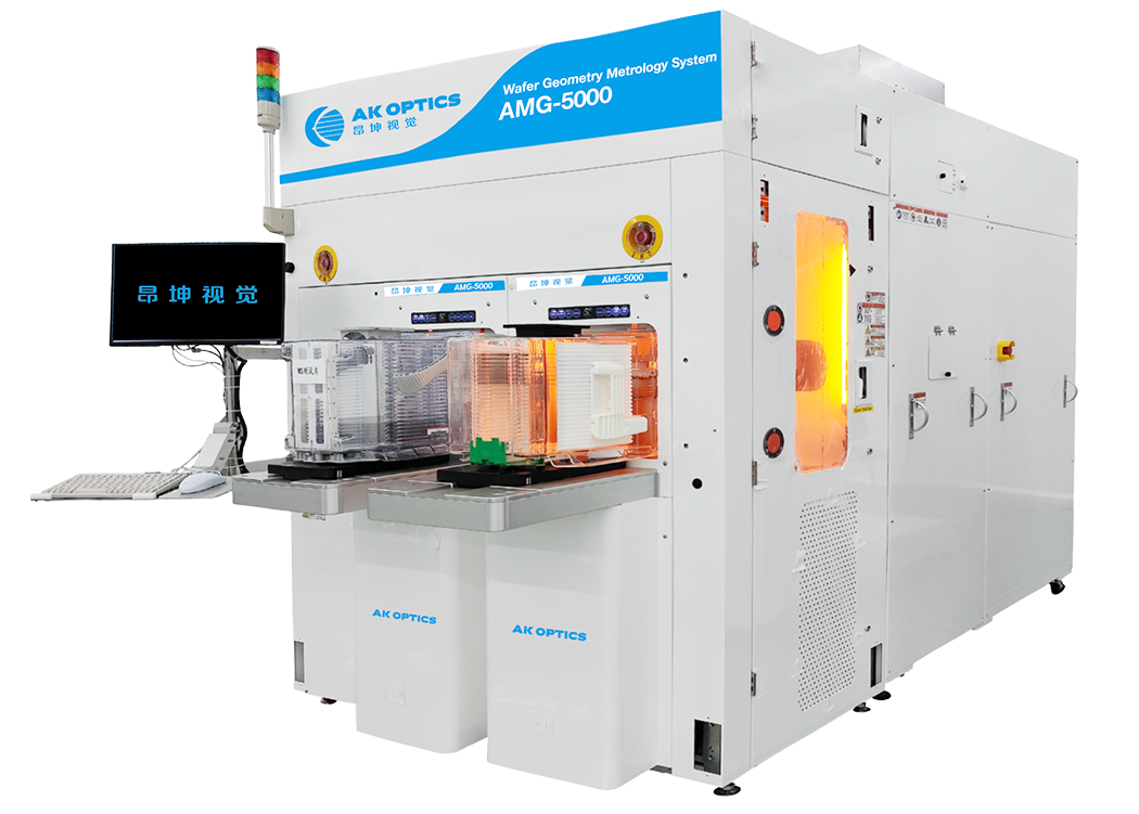
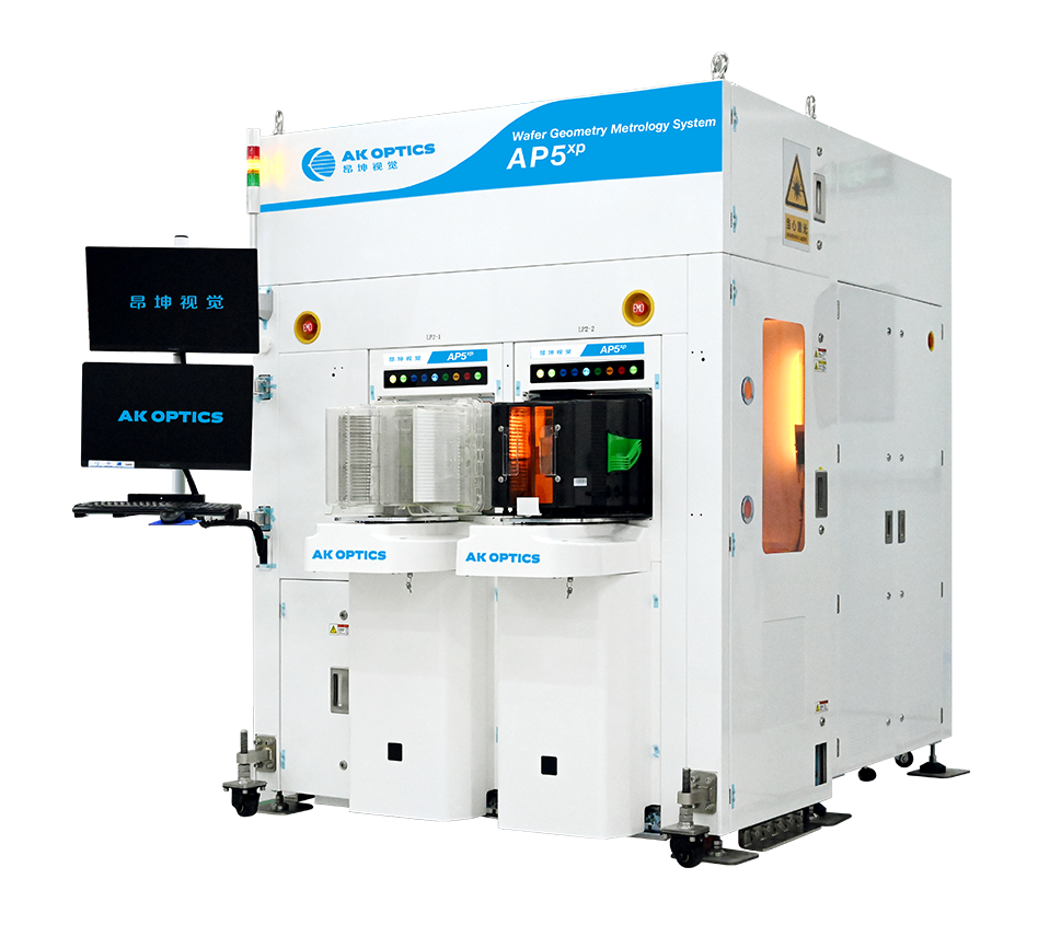
APG-5000 is AKO’s next-generation 300 mm silicon wafer metrology system, built on dual-side synchronous interferometric nanometrology.The system delivers optical resolution far beyond PWG5+ with sub-nanometer precision and seamless upgrade compatibility with PWG2+ and PWG5 platforms. Designed for patterned wafers, APG-5000 accurately measures thickness, flatness, shape, and dual-side nano-scale topography.The system provides advanced monitoring of wafer coating, CMP-induced warp, planar stress, higher-order deformation, and in-plane displacement (IPD), while supporting lithography Overlay error prediction and control. Deployed across R&D and HVM IC fabs, before and after wafer bonding and post-thinning, APG-5000 combines high precision with robust throughput to ensure reliable process control, maintain product quality, and maximize wafer and chip yield


  • Dual-side synchronous interferometric nano-metrology delivers ultimate precision for patterned wafer surface topography
  • Optical resolution well beyond PWG5+ fully supports metrology requirements for 7 nm advanced technology nodes
  • Production-ready, high-stability system maintains exceptional precision and throughput in both R&D and HVM environments
AWG-5000
Integrated Topography Metrology System

AWG-5000 is AKO’s integrated interferometric wafer geometry metrology system, designed for patterned wafers. It enables analysis and characterization of stress and its variation caused by coating, CMP, and wafer bonding, as well as in-plane displacement (IPD) resulting from higher-order deformation, critical for lithography Overlay error assessment. The system features high optical resolution, meeting EE = 1 mm advanced lithography inspection requirements. AWG-5000 supports Warpage, IPD, Stress, and LSC measurements, and accommodates multiple wafer placement modes including Chuck, air-bearing, and horizontal orientation, with 37 μm lateral resolution


  • Integrated interferometric geometry metrology for analyzing stress, IPD, and Overlay errors after coating, CMP, and wafer bonding
  • High optical resolution fully meets EE = 1 mm advanced lithography inspection requirements
  • Supports Chuck, air-bearing, and horizontal wafer placement, delivering 37um lateral resolution for versatile process monitoring
AP7XP
Unpatterned Wafer Defect Inspection System

AP7XP is innovatively designed and manufactured by AKO to deliver performance comparable to the KLA SP7XP. The system features a large field of view (FOV) and high numerical aperture (NA), with a minimum particle detection sensitivity of 12.5 nm and a lateral resolution of 0.7um.  Leveraging a TDI spiral line scan platform (similar to the SP7 configuration) and combining advanced AI withsmart algorithms, AP3 meets the stringent defect inspection requirements of high-volume wafer manufacturing (HVM) and IC FAB particle control,supporting technology nodes from 5 to 7 nm and effectively improving wafer and chip yield


  • Ultra-high sensitivity, capable of detecting particles down to 12 nm

  • Advanced TDI spiral scanning platform for precise and accurate measurements
  • Achieves exceptional throughput without compromising measurement precision
AP5XP
Unpatterned Wafer Defect Inspection Equipment

AP5XP is innovatively designed and manufactured by AKO to deliver performance comparable to the KLA SP7XP. The system features a large field of view (FOV) and high numerical aperture (NA), with a minimum particle detection sensitivity of 17 nm and a lateral resolution of 0.7um.  Leveraging a TDI spiral line scan platform (similar to the SP7 configuration) and combining advanced AI withsmart algorithms, AP5XP meets the stringent defect inspection requirements of high-volume wafer manufacturing (HVM) and IC FAB particle control, supporting technology nodes above14 nm and effectively improving wafer and chip yield


  • Ultra-high sensitivity, capable of detecting particles down to 12 nm

  • Advanced TDI spiral scanning platform for precise measurements

  • High throughput without compromisingmeasurement accuracy

AP3
Unpatterned Wafer Defect Inspection Equipment

AP3 is innovatively designed and manufactured by AKO to deliver performance comparable to the KLA SP7XP. The system features a large field of view (FOV) and high numerical aperture (NA), with a minimum particle detection sensitivity of19 nm and a lateral resolution of1.7um.Leveraging a TDI spiral line scan platform (similar to the SP7 configuration) and combining advanced AI withsmart algorithms, AP3 meets the stringent defect inspection requirements of high-volume wafer manufacturing (HVM) and IC FAB particle control, supporting technology nodes above 28 nm and effectively improving wafer and chip yield


  • Ultra-high sensitivity, capable of detecting particles down to 19nm

  • Advanced TDI spiral scanning platform for precise measurements

  • High throughput without compromising measurement accuracy


H series/ HB series
Patterned Wafer Bright/Dark Field Defect Inspection
Under construction
About Us
  • Established in Jan 2017, AK Optics is a leading optical inspection company in China for compound semiconductor and IC industries. Through years of technical innovation and continuous R&D efforts, AK optics is well known for its in-house designed optics and AI based platform which are widely adopted in the field of MOCVD in-situ monitoring, LED defect inspection, compound semiconductor defect inspection and IC metrology/defect inspection in mainland China and Taiwan.  
在线留言
以客户服务为中心,您的需求就是我们服务的方向,期待与您建立联系!