


2017
Angkun Vision was established.

2018
The shipment of Angkun MOCVD monitoring systems has exceeded 100 units.

2019
The cumulative shipment of AOI inspection equipment for LED lighting by Angkun has exceeded 300 units.

2020
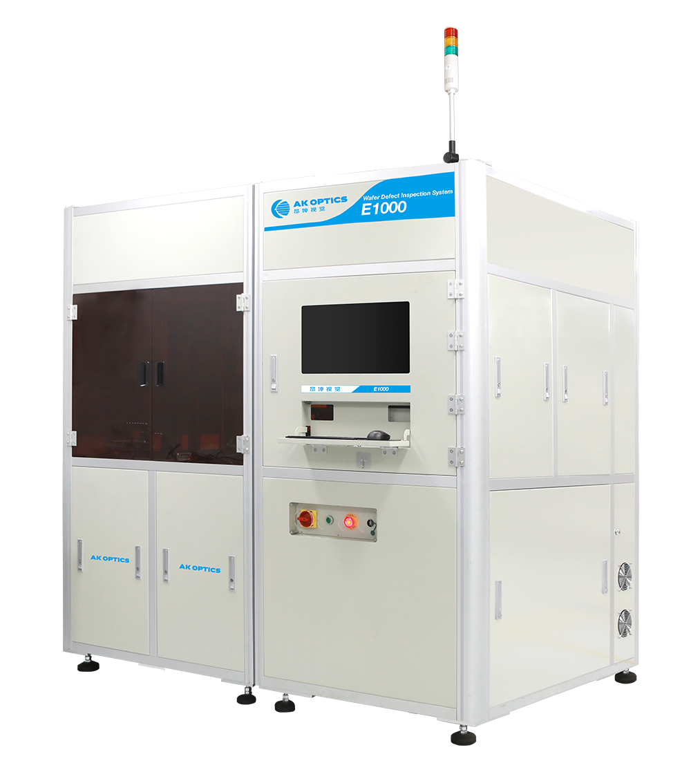
· For GaN, SiC substrate/epitaxial wafer defect detection equipment is officially shipped
· Angkun Vision was successfully selected as a "Specialized, Specialized, New" small and medium-sized enterprise in Beijing
· Angkun Vision was successfully selected as a "Specialized, Specialized, New" small and medium-sized enterprise in Beijing

2021
Angkun Vision was successfully selected as a national special and new key "Little Giant" enterprise
2022
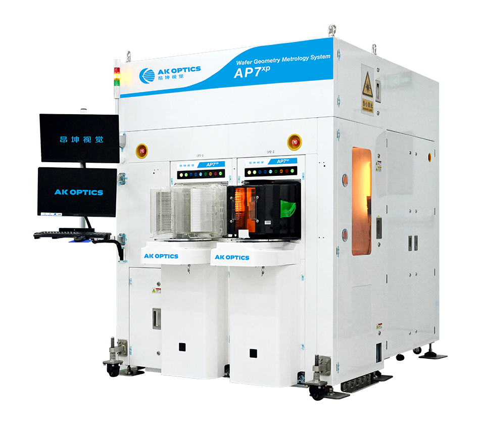
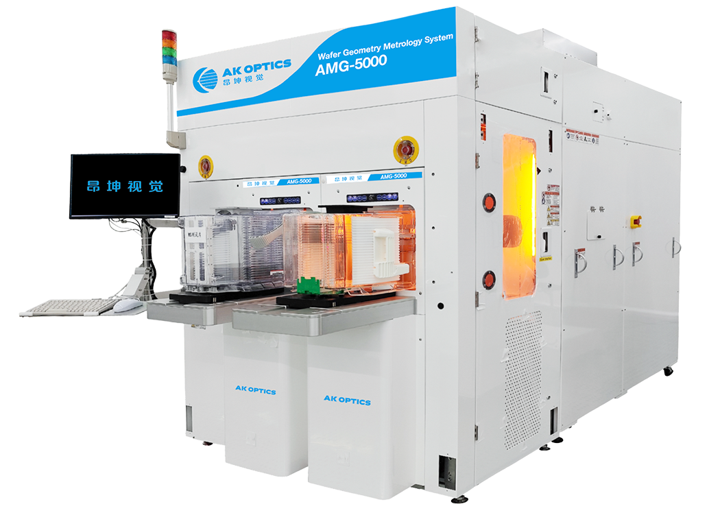
· Integrated circuit 12-inch detection equipment is officially shipped
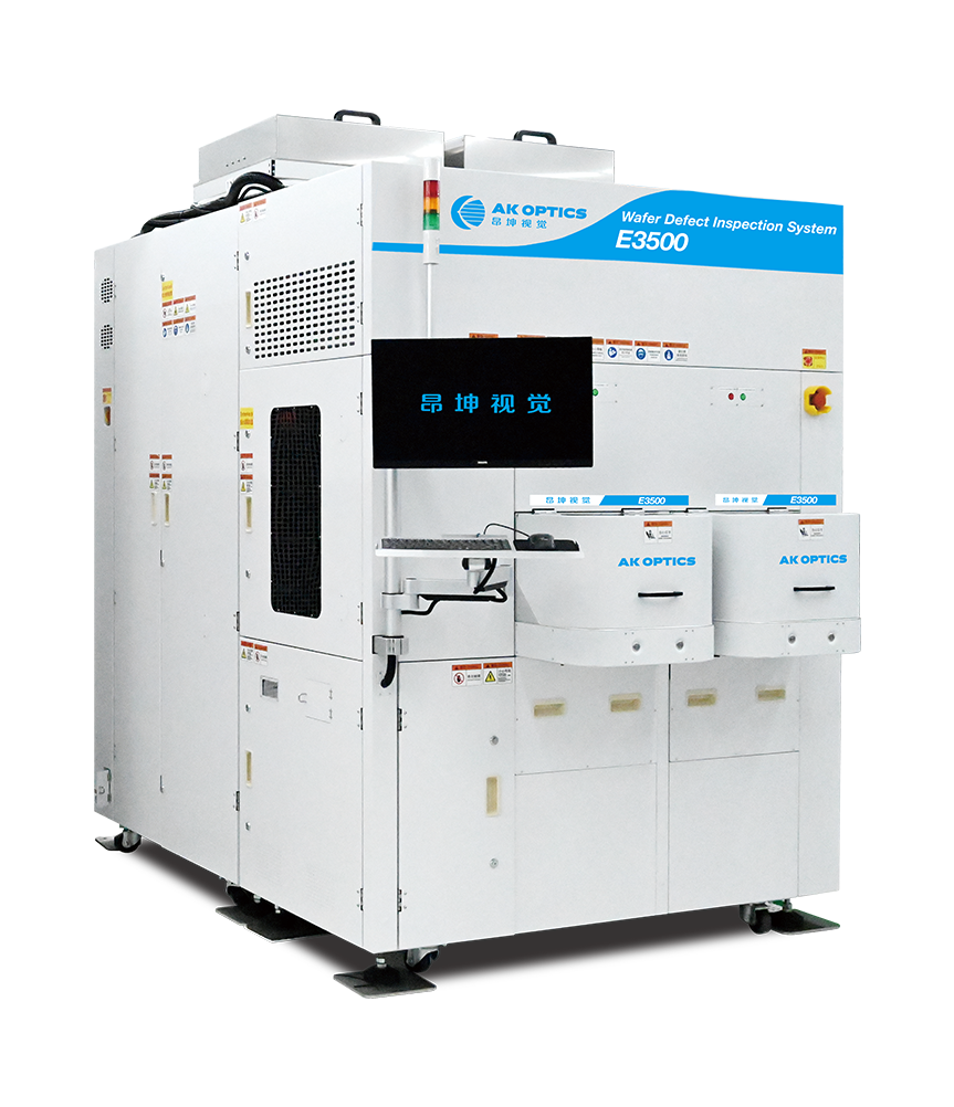
· Angkun compound detection equipment is shipped >100 units
2023
The second phase of the National Fund’s investment in Angkun Vision

2024
2025